

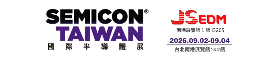
JSEDM will participate in SEMICON Taiwan 2026 from September 2 to September 4, 2026 at the Taipei Nangang Exhibition Center, Booth I3205, showcasing our latest technologies and applications in precision cutting of advanced materials.
As the semiconductor, advanced packaging, high-performance computing, and precision optics industries continue to evolve, the range of advanced materials being used is becoming increasingly diverse. Differences in electrical conductivity, hardness, brittleness, and thermal properties also create new challenges for precision machining.
At SEMICON Taiwan 2026, JSEDM will present “The Best Cutting Solutions for Your Materials” as our core theme, featuring two precision cutting technologies for different types of materials:
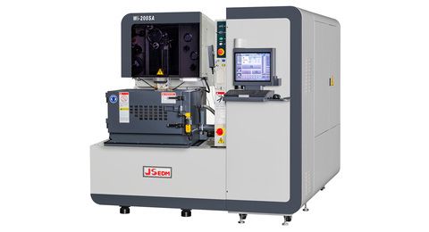
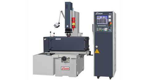
Wire EDM provides high-precision cutting and complex contour machining for a wide range of conductive materials;
Diamond Wire Saw extends precision cutting capabilities to non-conductive, hard and brittle materials, as well as precision optical materials.
By combining these two cutting technologies, JSEDM provides customers with a broader range of solutions for advanced material processing.
Conductive Material Applications|Wire EDM
For conductive metals and composite materials, JSEDM Wire EDM utilizes a non-contact electrical discharge machining process to achieve high dimensional accuracy, complex contours, and fine-feature machining.
At this exhibition, we will highlight three key application areas:
1. Data Center Thermal Management Modules
In response to the growing thermal management demands of AI, high-performance computing, and data centers, JSEDM will showcase precision cutting applications for high-thermal-conductivity materials such as copper, including heat dissipation structures, cooling fins, and related precision components.
2. Precision Semiconductor Component Manufacturing
For precision conductive components used in semiconductor equipment, JSEDM provides Wire EDM solutions for complex profiles, fine structures, and high-dimensional-accuracy machining.
3. Precision Mating Components
With the high-precision capabilities of Wire EDM, JSEDM can produce precisely matched male and female profiles, mating structures, and precision assembly components for applications requiring tight dimensional fit and accuracy.
In addition, JSEDM continues to conduct cutting tests on AlSiC (Aluminum Silicon Carbide) and other conductive composite materials with unique material properties, exploring their potential applications in advanced packaging, thermal management, and high-power semiconductor components.
Non-Conductive Material Applications|Diamond Wire Saw
For non-conductive, hard and brittle materials that cannot be processed by conventional EDM, JSEDM Diamond Wire Saw provides a low-cutting-force precision cutting solution, expanding the processing possibilities for advanced and specialty materials.
At this exhibition, we will highlight three key application areas:
1. Ultra-Low Expansion Glass Optical Components
For ultra-low-expansion glass-ceramics and dimensionally stable materials, JSEDM provides precision cutting solutions for applications in high-precision optics, astronomical observation, and precision equipment components.
2. Space Observation & High-Precision Sensing Components
For advanced hard and brittle materials used in astronomical observation, space optics, and high-precision sensing systems, JSEDM will demonstrate the precision cutting capabilities of Diamond Wire Saw for high-value advanced materials.
3. Semiconductor Substrate Slicing
For advanced materials including CVD Polycrystalline Diamond, Si₃N₄, Al₂O₃, and CVD Polycrystalline SiC , JSEDM provides precision slicing and material testing solutions designed to reduce cutting forces during the processing of hard and brittle materials while improving manufacturing flexibility.
From Material Testing to Small-Batch Production
JSEDM not only provides Wire EDM and Diamond Wire Saw machines, but also aims to serve as a technology partner for customers developing new material processing applications.
For advanced materials without established processing conditions, JSEDM works closely with customers throughout the R&D process, beginning with material cutting tests, machining parameter development, fixture design, and process validation to identify suitable processing methods. Depending on project requirements, we can also support small-batch trial production and machining services, helping customers shorten the development cycle from material validation to practical application.
From conductive to non-conductive materials, and from initial material testing to process development, JSEDM continues to expand the possibilities of precision cutting technology and provide optimized cutting solutions for a wide range of industries and advanced materials.
We sincerely invite you to visit JSEDM at Booth I3205 during SEMICON Taiwan 2026, September 2–4, 2026. Meet our team and discuss your material processing requirements as we explore new possibilities in precision cutting together.
SEMICON Taiwan 2026
Date|September 2–4, 2026
Venue|Taipei Nangang Exhibition Center
Booth|I3205
JSEDM — The Best Cutting Solutions for Your Materials
 Download